| CPC H01L 24/81 (2013.01) [B23K 1/008 (2013.01); H01L 23/49811 (2013.01); H01L 24/06 (2013.01); H01L 24/14 (2013.01); H01L 24/16 (2013.01); H01L 24/17 (2013.01); H01L 24/94 (2013.01); H01L 24/97 (2013.01); B23K 2101/40 (2018.08); H01L 2224/0603 (2013.01); H01L 2224/06136 (2013.01); H01L 2224/06155 (2013.01); H01L 2224/1403 (2013.01); H01L 2224/14136 (2013.01); H01L 2224/14155 (2013.01); H01L 2224/14177 (2013.01); H01L 2224/14515 (2013.01); H01L 2224/14517 (2013.01); H01L 2224/16145 (2013.01); H01L 2224/16146 (2013.01); H01L 2224/16148 (2013.01); H01L 2224/1703 (2013.01); H01L 2224/17136 (2013.01); H01L 2224/17155 (2013.01); H01L 2224/17177 (2013.01); H01L 2224/17517 (2013.01); H01L 2224/8183 (2013.01); H01L 2224/8192 (2013.01); H01L 2224/81143 (2013.01); H01L 2224/81191 (2013.01); H01L 2224/81192 (2013.01); H01L 2224/81193 (2013.01); H01L 2224/81815 (2013.01); H01L 2224/81906 (2013.01); H01L 2224/81907 (2013.01)] | 8 Claims |
|
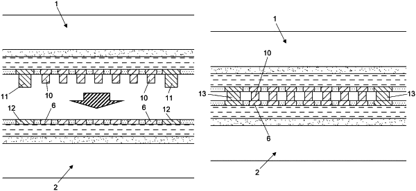
1. A method of bonding a first semiconductor component to a second semiconductor component, at least one of the components comprising a plurality of protruding metal contact structures, by bonding the plurality of protruding contact structures to corresponding protruding metal contact structures or metal contacts pads on the other component, the bonding taking place by direct metal to metal contact bonding, wherein
one of the components is provided with a plurality of dummy solder bumps for establishing solidified solder connections between the solder bumps and corresponding contact areas provided on the other component, the method comprising:
aligning the components so that the solder bumps are aligned to the corresponding contact areas;
realizing the solidified solder connections between the corresponding solders bumps and contact areas, wherein the solder bumps and contact areas are configured so that the protruding metal contact structures of one of the components are in physical contact with the corresponding protruding metal contact structures or the metal pads of the other component while not forming a metal bond, when the solidified solder connections are established, thereby obtaining an assembly of the first and second component bonded only through the solidified solder connections, wherein the solidified solder connections comprise an intermetallic compound (IMC); and
subjecting the assembly to a heat treatment for bonding the protruding metal contact structures to the corresponding metal structures or pads.
|