| CPC H01L 24/32 (2013.01) [H01L 23/3735 (2013.01); H02M 7/003 (2013.01)] | 14 Claims |
|
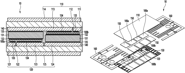
1. A power module comprising:
a first substrate comprising a first metal plate disposed at a first side of the first substrate;
a second substrate spaced apart from the first substrate, the second substrate comprising a second metal plate that is disposed at a second side of the second substrate and faces the first metal plate; and
a plurality of power elements disposed between the first substrate and the second substrate, wherein the plurality of power elements comprise insulated gate bipolar transistor (IGBT) semiconductor elements, each of the plurality of power elements comprising:
a first electrode disposed at a first surface of each of the plurality of power elements, wherein the first electrode comprises a gate electrode and an emitter electrode of one of the IGBT semiconductor elements, and
a second electrode disposed at a second surface of each of the plurality of power elements, wherein the second electrode comprises a collector electrode of the one of the IGBT semiconductor elements,
wherein the plurality of power elements comprise:
a first power element having the gate electrode and the emitter electrode that are coupled to the second metal plate,
a first spacer disposed between the first metal plate and the first power element and coupled to the first metal plate, wherein the first spacer is coupled to the collector electrode of the first power element,
a second power element having the gate electrode and the emitter electrode that are coupled to the first metal plate, and
a second spacer disposed between the second power element and the second metal plate and coupled to the second metal plate, wherein the second spacer is coupled to the collector electrode of the second power element,
wherein each of the first and second spacers has a thickness predetermined to compensate a thickness difference between the first and second power elements, the first and second power elements having thicknesses different from each other.
|