| CPC H01L 24/25 (2013.01) [H01L 23/3107 (2013.01); H01L 23/3114 (2013.01); H01L 23/50 (2013.01); H01L 23/5389 (2013.01); H01L 24/19 (2013.01); H01L 24/24 (2013.01); H01L 25/16 (2013.01); H01L 25/18 (2013.01); H01L 21/568 (2013.01); H01L 23/3128 (2013.01); H01L 2224/04105 (2013.01); H01L 2224/12105 (2013.01); H01L 2224/16227 (2013.01); H01L 2224/2501 (2013.01); H01L 2224/2505 (2013.01); H01L 2224/255 (2013.01); H01L 2224/2512 (2013.01); H01L 2224/73209 (2013.01); H01L 2224/81005 (2013.01); H01L 2224/92133 (2013.01); H01L 2924/10253 (2013.01); H01L 2924/12042 (2013.01); H01L 2924/141 (2013.01); H01L 2924/1431 (2013.01); H01L 2924/1461 (2013.01); H01L 2924/15151 (2013.01); H01L 2924/15192 (2013.01); H01L 2924/15747 (2013.01); H01L 2924/18161 (2013.01); H01L 2924/18162 (2013.01)] | 24 Claims |
|
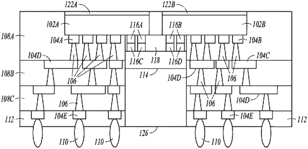
1. A semiconductor package, comprising:
a first dielectric layer including through vias therein, the through vias having a first pitch;
a high density interconnect structure in the first dielectric layer, the high density interconnect structure between a first portion and a second portion of the through vias in the first dielectric layer, the high density interconnect structure having interconnect pads having a second pitch less than the first pitch;
a second dielectric layer on the first dielectric layer, the second dielectric layer having a top surface;
a first die in the second dielectric layer, the first die coupled to the first portion of the through vias in the first dielectric layer and coupled to a first portion of the interconnect pads of the high density interconnect structure, and the first die having a top surface co-planar with the top surface of the second dielectric layer; and
a second die in the second dielectric layer, the second die coupled to the second portion of the through vias in the first dielectric layer and coupled to a second portion of the interconnect pads of the high density interconnect structure, wherein the interconnect pads of the high density interconnect structure face towards the first die and the second die.
|