| CPC H01L 24/24 (2013.01) [H01L 23/3135 (2013.01); H01L 23/481 (2013.01); H01L 24/25 (2013.01); H01L 25/0652 (2013.01); H01L 25/0657 (2013.01); H01L 25/105 (2013.01); H01L 25/50 (2013.01); H01L 23/5385 (2013.01); H01L 24/08 (2013.01); H01L 24/16 (2013.01); H01L 24/32 (2013.01); H01L 24/73 (2013.01); H01L 2224/08145 (2013.01); H01L 2224/16145 (2013.01); H01L 2224/2402 (2013.01); H01L 2224/24011 (2013.01); H01L 2224/24101 (2013.01); H01L 2224/24175 (2013.01); H01L 2224/25171 (2013.01); H01L 2224/32145 (2013.01); H01L 2224/73204 (2013.01); H01L 2224/73259 (2013.01); H01L 2224/73267 (2013.01); H01L 2225/06568 (2013.01); H01L 2225/1035 (2013.01); H01L 2225/1041 (2013.01); H01L 2225/1058 (2013.01)] | 20 Claims |
|
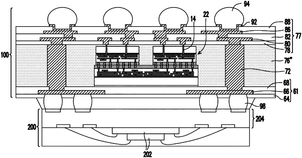
1. A package structure, comprising:
a first semiconductor die, wherein the first semiconductor die comprises a first bonding structure;
a second semiconductor die, wherein the second semiconductor die comprises a second bonding structure, the first semiconductor die being stacked over and electrically connected to the second semiconductor die, wherein the first bonding structure is bonded to the second bonding structure;
an insulating encapsulant laterally encapsulating the first semiconductor die and the second semiconductor die, the insulating encapsulant comprising a first encapsulation portion and a second encapsulation portion continuous with the first encapsulation portion, the first encapsulation portion being disposed on the second semiconductor die and laterally encapsulating the first semiconductor die, and the second encapsulation portion laterally encapsulating the first encapsulation portion and the second semiconductor die; and
a first redistribution circuit structure disposed on the first semiconductor die, the second semiconductor die, and a first surface of the insulating encapsulant, wherein the first redistribution circuit structure is electrically connected to the first semiconductor die.
|