| CPC H01L 24/13 (2013.01) [H01L 23/3114 (2013.01); H01L 23/49548 (2013.01); H01L 23/49582 (2013.01); H01L 23/5226 (2013.01); H01L 23/5283 (2013.01); H01L 24/03 (2013.01); H01L 24/05 (2013.01); H01L 24/06 (2013.01); H01L 23/3107 (2013.01); H01L 23/53223 (2013.01); H01L 23/53238 (2013.01); H01L 23/562 (2013.01); H01L 24/29 (2013.01); H01L 24/32 (2013.01); H01L 24/45 (2013.01); H01L 24/48 (2013.01); H01L 24/49 (2013.01); H01L 24/73 (2013.01); H01L 24/83 (2013.01); H01L 2224/02166 (2013.01); H01L 2224/04042 (2013.01); H01L 2224/05012 (2013.01); H01L 2224/05147 (2013.01); H01L 2224/05155 (2013.01); H01L 2224/05582 (2013.01); H01L 2224/05655 (2013.01); H01L 2224/05664 (2013.01); H01L 2224/1318 (2013.01); H01L 2224/13018 (2013.01); H01L 2224/1357 (2013.01); H01L 2224/13082 (2013.01); H01L 2224/13147 (2013.01); H01L 2224/13166 (2013.01); H01L 2224/13171 (2013.01); H01L 2224/13176 (2013.01); H01L 2224/13181 (2013.01); H01L 2224/13184 (2013.01); H01L 2224/13647 (2013.01); H01L 2224/293 (2013.01); H01L 2224/29101 (2013.01); H01L 2224/32245 (2013.01); H01L 2224/45124 (2013.01); H01L 2224/45144 (2013.01); H01L 2224/45147 (2013.01); H01L 2224/48091 (2013.01); H01L 2224/48227 (2013.01); H01L 2224/48247 (2013.01); H01L 2224/48465 (2013.01); H01L 2224/49171 (2013.01); H01L 2224/73265 (2013.01); H01L 2224/83439 (2013.01); H01L 2224/83801 (2013.01); H01L 2924/01022 (2013.01); H01L 2924/01024 (2013.01); H01L 2924/01028 (2013.01); H01L 2924/01029 (2013.01); H01L 2924/01042 (2013.01); H01L 2924/01044 (2013.01); H01L 2924/01046 (2013.01); H01L 2924/01073 (2013.01); H01L 2924/01074 (2013.01); H01L 2924/04941 (2013.01); H01L 2924/181 (2013.01)] | 21 Claims |
|
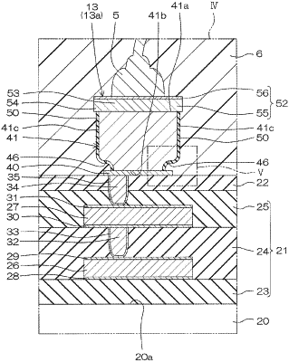
1. A semiconductor device comprising:
an insulating layer;
a first metal layer formed over a part of region of a surface of the insulating layer; and
a bonding pad formed on part of a principal surface of the first metal layer, wherein the bonding pad includes a Cu electrode layer, a nickel layer, and a surface metal layer formed from bottom to top; and
wherein a surface of the surface metal layer is exposed from the insulating layer for connecting a bonding wire on the surface, a thickness of the surface metal layer is thinner than a thickness of the nickel layer, and a thickness of the nickel layer is thinner than a thickness of the Cu electrode layer,
wherein a width of an outermost surface of the Cu electrode layer is wider than a width of a bottom surface of the Cu electrode layer.
|