| CPC H01L 24/06 (2013.01) [G06F 30/392 (2020.01); G06F 30/398 (2020.01); H01L 21/78 (2013.01); H01L 23/522 (2013.01); H01L 23/528 (2013.01); H01L 23/5226 (2013.01); H01L 23/5329 (2013.01); H01L 23/562 (2013.01); H01L 23/585 (2013.01); H01L 24/03 (2013.01); H01L 29/0649 (2013.01); H01L 22/34 (2013.01); H01L 23/3114 (2013.01); H01L 23/525 (2013.01); H01L 23/53214 (2013.01); H01L 23/53228 (2013.01); H01L 23/53233 (2013.01); H01L 23/53257 (2013.01); H01L 23/53261 (2013.01); H01L 23/544 (2013.01); H01L 2223/5446 (2013.01); H01L 2223/54426 (2013.01); H01L 2224/0239 (2013.01); H01L 2224/02311 (2013.01); H01L 2224/02371 (2013.01); H01L 2224/0345 (2013.01); H01L 2224/03452 (2013.01); H01L 2224/03464 (2013.01); H01L 2224/03614 (2013.01); H01L 2224/03827 (2013.01); H01L 2224/03848 (2013.01); H01L 2224/0401 (2013.01); H01L 2224/04042 (2013.01); H01L 2224/05111 (2013.01); H01L 2224/05124 (2013.01); H01L 2224/05144 (2013.01); H01L 2224/05147 (2013.01); H01L 2224/05155 (2013.01); H01L 2224/061 (2013.01); H01L 2924/01013 (2013.01); H01L 2924/01029 (2013.01); H01L 2924/2011 (2013.01); H01L 2924/20106 (2013.01); H01L 2924/20107 (2013.01); H01L 2924/20108 (2013.01); H01L 2924/20109 (2013.01); H01L 2924/3512 (2013.01); H01L 2924/35121 (2013.01)] | 20 Claims |
|
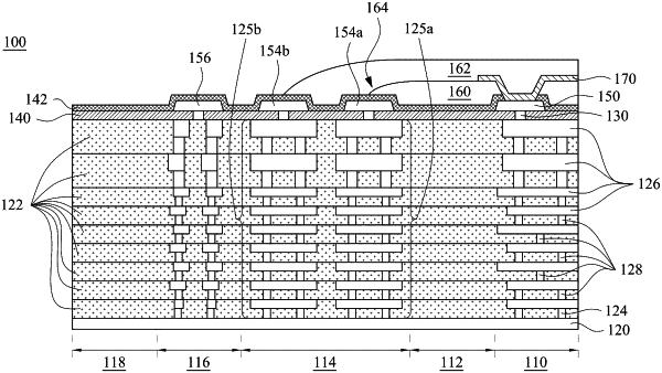
1. A semiconductor structure comprising:
a first contact pad over an interconnect structure;
a second contact pad over the interconnect structure, wherein the second contact pad is electrically separated from the first contact pad; and
a first buffer layer over the first contact pad, wherein the first buffer layer is partially over the second contact pad, and an edge of the second contact pad farthest from the first contact pad extends beyond the first buffer layer.
|