| CPC H01L 24/01 (2013.01) [H01L 21/2007 (2013.01); H01L 23/5222 (2013.01); G02B 6/1225 (2013.01); G02B 6/305 (2013.01); G02B 2006/12061 (2013.01)] | 20 Claims |
|
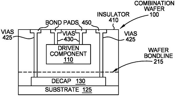
1. A combination wafer, comprising:
a first wafer comprising an optical modulator; and
a second wafer comprising a decoupling capacitor, wherein the first wafer and the second wafer are directly bonded along a wafer bond line,
wherein the first wafer comprises a plurality of vias that electrically connect the decoupling capacitor in the second wafer to bond pads disposed on a first side of the first wafer that is opposite the wafer bond line,
wherein the second wafer is a semiconductor wafer and the first wafer comprises a photonic chip that includes the optical modulator.
|