| CPC H01L 23/62 (2013.01) [H01L 23/5256 (2013.01); H01H 2085/0283 (2013.01)] | 15 Claims |
|
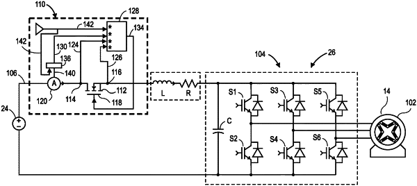
1. A solid-state fuse device, comprising:
a switch having a first switch terminal, a second switch terminal, and a switch gate terminal;
a current sensor having a first current measuring port connected to a traction battery, a second current measuring port connected to the switch, and an overcurrent signal output port, wherein the current sensor is configured to output an overcurrent signal to the overcurrent signal output port in response to determining that an overcurrent has been measured by the current sensor for at least a tunable delay time period;
a latch having a first latch input port configured to receive a reset signal, a second latch input port connected to the overcurrent signal output port of the current sensor, and a latch output port, wherein the latch is configured to output a latch state signal indicative of a state maintained by the latch to the latch output port, and wherein the latch is configured to transition from a first state to a second state when the overcurrent signal exceeds a predetermined overcurrent threshold and output the latch state signal indicative of the second state to the latch output port; and
a gate driver having a first gate driver input port configured to receive the reset signal, a second gate driver input port connected to the latch output port, a third gate driver input port connected to the first switch terminal, a fourth gate driver input port connected to the second switch terminal, and a gate driver output port connected to the switch gate terminal, wherein the gate driver is configured to:
transition the switch from a closed state to an open state when an overcurrent measurement exceeds the predetermined overcurrent threshold for at least the tunable delay time period, wherein the overcurrent measurement is determined based at least in part on the latch state signal received at the second gate driver input port; and
transition the switch from the closed state to the open state when a voltage drop across the switch exceeds a predetermined saturation voltage threshold, wherein the voltage drop across the switch is determined based at least in part on a voltage difference between the third gate driver input port and the fourth gate driver input port; and
transition the switch from the open state to the closed state when the reset signal is received at the first gate driver input port.
|