| CPC H01L 23/562 (2013.01) [H01L 21/4825 (2013.01); H01L 21/565 (2013.01); H01L 21/78 (2013.01); H01L 22/12 (2013.01); H01L 23/3114 (2013.01); H01L 23/4952 (2013.01); H01L 23/49503 (2013.01); H01L 23/49562 (2013.01); H01L 23/544 (2013.01); H01L 24/03 (2013.01); H01L 24/05 (2013.01); H01L 24/06 (2013.01); H01L 24/09 (2013.01); H01L 24/46 (2013.01); H01L 22/32 (2013.01); H01L 23/3192 (2013.01); H01L 24/02 (2013.01); H01L 24/45 (2013.01); H01L 2223/54486 (2013.01); H01L 2224/02166 (2013.01); H01L 2224/04042 (2013.01); H01L 2224/05552 (2013.01); H01L 2224/05553 (2013.01); H01L 2224/05567 (2013.01); H01L 2224/06133 (2013.01); H01L 2224/06155 (2013.01); H01L 2224/45144 (2013.01); H01L 2224/48091 (2013.01); H01L 2224/48247 (2013.01); H01L 2224/4905 (2013.01); H01L 2924/13091 (2013.01); H01L 2924/181 (2013.01)] | 40 Claims |
|
1. A semiconductor chip comprising:
a first pad;
a first lead-out wiring portion integrally formed with the first pad, the first lead-out wiring portion connected to a lower-layer wiring through a first contact;
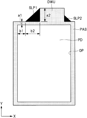
a sloped portion formed on a connection part between the first pad and the first lead-out wiring portion;
a surface protective film covering the first lead-out wiring portion, the surface protective film on which a first opening is formed to expose a part of a surface of the first pad; and
a second pad formed next to the first pad along an edge side of the semiconductor chip,
wherein a central position of a width of the first lead-out wiring portion is shifted relative to a central position of a side to which the first lead-out wiring portion is connected among a plurality of sides making up the first pad, and
wherein a connection angle of the connection part between the first pad and the first lead-out wiring portion is comprised of obtuse angles formed at two spots,
wherein a second opening is formed on the surface protective film to expose a part of a surface of the second pad, and
wherein, in plan view, a difference between a size of the first pad and a size of the second pad is larger than a difference between a size of the first opening and a size of the second opening.
|