| CPC H01L 23/552 (2013.01) [H01L 23/49811 (2013.01); H01L 24/06 (2013.01); H01L 24/13 (2013.01); H01L 24/16 (2013.01); H01L 24/17 (2013.01); H01L 24/48 (2013.01); H01L 24/49 (2013.01); H01L 24/73 (2013.01); H01L 25/03 (2013.01); H01L 25/0652 (2013.01); H01L 25/0655 (2013.01); H01L 25/0657 (2013.01); H01L 25/105 (2013.01); H01L 24/29 (2013.01); H01L 24/32 (2013.01); H01L 2224/04042 (2013.01); H01L 2224/05599 (2013.01); H01L 2224/1134 (2013.01); H01L 2224/12105 (2013.01); H01L 2224/131 (2013.01); H01L 2224/13076 (2013.01); H01L 2224/13082 (2013.01); H01L 2224/16145 (2013.01); H01L 2224/16227 (2013.01); H01L 2224/16265 (2013.01); H01L 2224/17051 (2013.01); H01L 2224/17181 (2013.01); H01L 2224/215 (2013.01); H01L 2224/2919 (2013.01); H01L 2224/32225 (2013.01); H01L 2224/45015 (2013.01); H01L 2224/48105 (2013.01); H01L 2224/48227 (2013.01); H01L 2224/48472 (2013.01); H01L 2224/4942 (2013.01); H01L 2224/73204 (2013.01); H01L 2224/73207 (2013.01); H01L 2224/73227 (2013.01); H01L 2224/73253 (2013.01); H01L 2224/73259 (2013.01); H01L 2224/73265 (2013.01); H01L 2224/73267 (2013.01); H01L 2224/85444 (2013.01); H01L 2224/85455 (2013.01); H01L 2225/06513 (2013.01); H01L 2225/06517 (2013.01); H01L 2225/1023 (2013.01); H01L 2225/1052 (2013.01); H01L 2924/00014 (2013.01); H01L 2924/01322 (2013.01); H01L 2924/1205 (2013.01); H01L 2924/1206 (2013.01); H01L 2924/1207 (2013.01); H01L 2924/181 (2013.01); H01L 2924/19105 (2013.01); H01L 2924/19107 (2013.01); H01L 2924/2075 (2013.01); H01L 2924/20751 (2013.01); H01L 2924/20754 (2013.01); H01L 2924/3025 (2013.01)] | 28 Claims |
|
1. An apparatus, comprising:
a package substrate of a system-in-package having an upper surface and a lower surface opposite the upper surface and having at least one conductive element on the upper surface;
a first and a second microelectronic device coupled to the upper surface of the substrate;
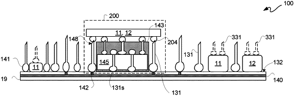
an EMI shield covering the first microelectronic device, the EMI shield comprising at least one side portion and a top portion, the at least one side portion including wire bond wires having first ends bonded to the at least one conductive element, at least two wire bond wires of the wire bond wires having first ends bonded to the same conductive element, the wire bond wires arranged in a preselected manner for one or more frequencies associated with an interference, the wire bond wires positioned on at least one side of the first microelectronic device to substantially shield the interference at the one or more frequencies relative to the first microelectronic device;
the second microelectronic device separated from the first microelectronic device by the at least one side portion or the top portion of the EMI shield, wherein the second microelectronic device is a passive device; and
a third microelectronic device separated from the first microelectronic device by the at least one side portion or the top portion of the EMI shield, wherein the third microelectronic device is an active device.
|