| CPC H01L 23/525 (2013.01) [H01L 21/76802 (2013.01); H01L 21/76877 (2013.01); H01L 21/823871 (2013.01); H01L 23/5226 (2013.01); H01L 23/5228 (2013.01); H10N 70/231 (2023.02)] | 8 Claims |
|
1. A method for forming a semiconductor device, comprising:
forming a plurality of conductive lines as a part of a first wiring level of the semiconductor device, the first wiring level being positioned over a first level having a plurality of transistor devices, the plurality of conductive lines extending parallel to the first level;
forming a programmable vertical bridge that is positioned below the plurality of conductive lines and extends perpendicular to the first level, the programmable vertical bridge physically connecting a first conductive line of the plurality of conductive lines in the first wiring level, the programmable vertical bridge being formed based on a first material that changes phase between a conductive state and a non-conductive state according to a current pattern delivered to the programmable vertical bridge; and
forming a first conductive vertical bridge that is positioned below the plurality of the conductive lines and extends perpendicular to the first level, the first conductive vertical bridge being spaced apart from the programmable vertical bridge and physically connecting a second conductive line of the plurality of the conductive lines, wherein forming the programmable vertical bridge comprises:
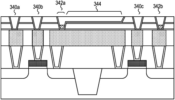
forming a first relief pattern in a dielectric material positioned over a substrate, the first relief pattern having a plurality of vertical openings;
depositing the first material to fill the vertical openings of the first relief pattern;
covering a portion of the first material that fills one of the plurality of vertical openings by a first mask to form the programmable vertical bridge;
removing a uncovered portion of the first material that fills other vertical openings of the plurality of vertical openings;
removing the first mask; and
filling the other vertical openings of the plurality of vertical openings with a conductive material to form a plurality of conductive vertical interconnects that includes the first conductive vertical bridge.
|