| CPC H01L 23/49833 (2013.01) [H01L 21/4853 (2013.01); H01L 23/49816 (2013.01); H01L 23/49838 (2013.01); H01L 24/16 (2013.01); H01L 24/32 (2013.01); H01L 24/73 (2013.01); H01L 24/81 (2013.01); H01L 2224/16227 (2013.01); H01L 2224/32225 (2013.01); H01L 2224/73204 (2013.01); H01L 2924/37001 (2013.01)] | 20 Claims |
|
1. A package structure, comprising:
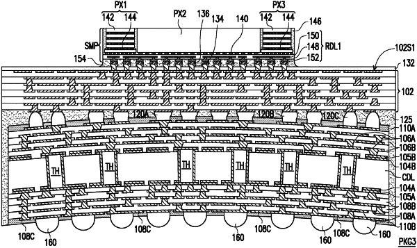
a redistribution structure having a first surface and a second surface opposite to the first surface;
a semiconductor package disposed on the first surface and electrically connected to the redistribution structure;
a plurality of core substrates disposed on the second surface and electrically connected to the redistribution structure, wherein the plurality of core substrates partially covers the second surface of the redistribution structure, and each of the plurality of core substrates comprises:
a core layer;
a first interconnection layer and a second interconnection layer disposed on two opposing surfaces of the core layer; and
a plurality of conductive terminals disposed on the first interconnection layer and sandwiched between the second surface of the redistribution structure and the first interconnection layer, wherein a height of the plurality of conductive terminals decreases from a boundary region of the first interconnection layer to a central region of the first interconnection layer; and
an insulating encapsulant encapsulating the plurality of core substrates, wherein sidewalls of the insulating encapsulant are aligned with sidewalls of the redistribution structure, and the insulating encapsulant covers and surround the plurality of conductive terminals with decreasing height.
|