| CPC H01L 23/49827 (2013.01) [H01L 21/76816 (2013.01); H01L 21/76831 (2013.01)] | 20 Claims |
|
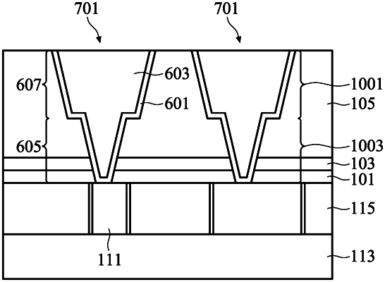
1. A method of manufacturing a semiconductor device, the method comprising:
forming a dielectric layer over a first etch stop layer over a conductive feature;
forming an anti-reflective layer over the dielectric layer;
forming a first hard mask over the anti-reflective layer;
patterning the first hard mask to have a first opening larger than a second opening through the anti-reflective layer;
forming a first via opening and a first trench opening through the dielectric layer, wherein the forming the first via opening and the first trench opening is performed by etching through both the first opening and the second opening with a single etching process;
removing the first hard mask; and
removing a portion of the first etch stop layer through the first via opening, wherein after the removing the portion of the first etch stop layer has been stopped the via opening has a first profile angle of between about 70° and about 80°, wherein the removing the portion of the first etch stop layer also rounds a corner of the anti-reflective layer.
|