| CPC H01L 23/3675 (2013.01) [H01L 21/486 (2013.01); H01L 21/4853 (2013.01); H01L 21/4878 (2013.01); H01L 21/4882 (2013.01); H01L 21/563 (2013.01); H01L 21/67092 (2013.01); H01L 23/3185 (2013.01); H01L 23/40 (2013.01); H01L 23/49827 (2013.01); H01L 23/562 (2013.01); H01L 24/16 (2013.01); H01L 25/0655 (2013.01); H01L 2224/16225 (2013.01)] | 20 Claims |
|
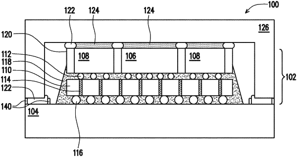
1. A semiconductor device comprising:
an interposer substrate bonded to a package substrate;
a device die bonded to the interposer substrate;
an encapsulant surrounding the device die;
an underfill between the device die and the interposer substrate, wherein the underfill surrounds sidewalls of the interposer substrate;
an adhesive on the package substrate and a surface of the encapsulant opposite the package substrate;
a thermal interface material on a surface of the device die opposite the package substrate; and
a lid over the device die and the package substrate, wherein the lid contacts the adhesive and the thermal interface material, and wherein the adhesive has a thickness between the lid and the encapsulant greater than a thickness of the thermal interface material between the lid and the device die.
|