| CPC H01L 23/13 (2013.01) [H01L 23/49833 (2013.01); H01L 23/5384 (2013.01); H01L 23/5385 (2013.01); H01L 24/16 (2013.01); H01L 24/17 (2013.01); H01L 25/50 (2013.01); H01L 25/18 (2013.01); H01L 2224/16148 (2013.01); H01L 2224/16238 (2013.01)] | 20 Claims |
|
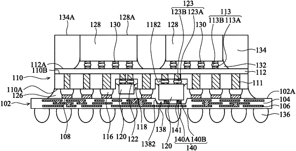
1. A package structure, comprising:
a package substrate;
an interposer substrate disposed over the package substrate, wherein the interposer substrate includes a silicon substrate, and wherein the interposer substrate has a bottom surface facing and adjacent to the package substrate, a top surface opposite the bottom surface, a first cavity formed on the top surface, and a second cavity formed on the bottom surface;
a first semiconductor device disposed on the top surface of the interposer substrate;
a second semiconductor device disposed in the first cavity and electrically connected to the first semiconductor device and/or the interposer substrate; and
a third semiconductor device disposed in the second cavity,
wherein the package substrate has a top surface facing and adjacent to the interposer substrate, and a third cavity is formed on the top surface of the package substrate and aligned with the second cavity of the interposer substrate, wherein the third cavity is configured to accommodate the third semiconductor device.
|