| CPC H01L 21/823821 (2013.01) [H01L 21/823481 (2013.01); H01L 21/823807 (2013.01); H01L 21/823878 (2013.01); H01L 27/0924 (2013.01); H01L 29/1054 (2013.01); H01L 29/7843 (2013.01); H01L 29/7846 (2013.01); H01L 21/0217 (2013.01); H01L 21/02164 (2013.01); H01L 21/02271 (2013.01); H01L 21/31105 (2013.01); H01L 21/31144 (2013.01); H01L 21/823892 (2013.01); H01L 27/0928 (2013.01)] | 20 Claims |
|
1. A semiconductor device, comprising:
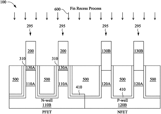
a first transistor formed over a first well, wherein the first transistor includes a first fin structure;
a second transistor formed over a second well, wherein the first well and the second well are doped oppositely, the second transistor includes a second fin structure that contains silicon and doped silicon;
an isolation structure formed over the first well, over the second well, and between the first transistor and the second transistor;
a first number of liner layers disposed between the first transistor and the isolation structure; and
a second number of liner layers disposed between the second transistor and the isolation structure, wherein the second number is less than the first number, and wherein an innermost side surface of the second number of liner layers is in direct contact with a portion, but not all, of a silicon side surface of the second fin structure, and wherein the innermost side surface of the second number of liner layers is in direct contact with an entirety of a doped silicon side surface of the second fin structure.
|