| CPC H01L 21/823481 (2013.01) [H01L 21/823412 (2013.01); H01L 21/823431 (2013.01); H01L 21/823437 (2013.01); H01L 21/823821 (2013.01); H01L 21/823878 (2013.01); H01L 29/0673 (2013.01); H01L 29/42392 (2013.01); H01L 29/66795 (2013.01); H01L 29/785 (2013.01); H01L 29/78696 (2013.01)] | 20 Claims |
|
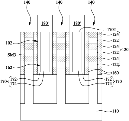
9. A method for manufacturing a semiconductor device, comprising:
forming a semiconductor fin over a substrate;
forming an isolation feature adjacent the semiconductor fin;
recessing the isolation feature to form a first recess;
forming a metal-containing compound mask in the first recess;
recessing the semiconductor fin to expose a sidewall of the metal-containing compound mask;
depositing a stress layer over the recessed the semiconductor fin and in contact with the sidewall of the metal-containing compound mask; and
annealing the metal-containing compound mask.
|