| CPC H01L 21/76898 (2013.01) [H01L 21/3205 (2013.01); H01L 21/768 (2013.01); H01L 21/76831 (2013.01); H01L 23/12 (2013.01); H01L 23/13 (2013.01); H01L 23/14 (2013.01); H01L 23/481 (2013.01); H01L 23/522 (2013.01); H01L 23/53209 (2013.01); H05K 1/11 (2013.01); H05K 3/40 (2013.01)] | 15 Claims |
|
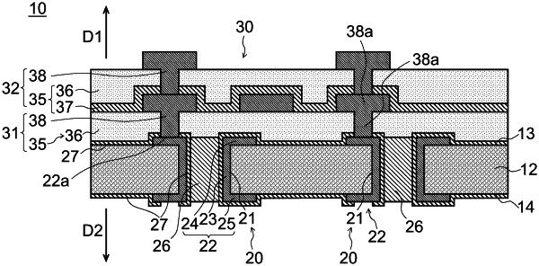
1. A through electrode substrate comprising:
a substrate including a first surface positioned on a first side, and a second surface positioned on a second side opposite to the first side, the substrate being provided with a through hole;
a through electrode having a sidewall portion extending along a sidewall of the through hole, and a first portion positioned on the first surface of the substrate and connected to the sidewall portion;
an inorganic film that at least partially covers the first portion of the through electrode from the first side and is provided with an opening positioned on the first portion; and
a first wiring structure including at least a first wiring layer having an insulation layer that is positioned to the first side of the inorganic film and includes at least an organic layer provided with an opening communicating with the opening of the inorganic film, and an electroconductive layer connected to the first portion of the through electrode through the opening of the inorganic film and the opening of the insulation layer.
|