| CPC H01L 21/76858 (2013.01) [H01L 21/7684 (2013.01); H01L 21/76802 (2013.01); H01L 21/76846 (2013.01); H01L 21/76877 (2013.01); H01L 23/5226 (2013.01); H01L 23/53238 (2013.01)] | 10 Claims |
|
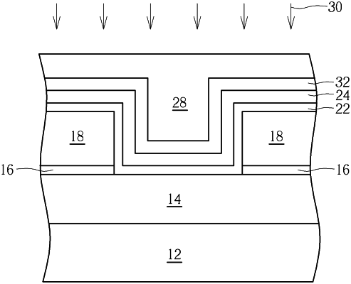
1. A method for fabricating semiconductor device, comprising:
forming a dielectric layer on a substrate;
forming a trench in the dielectric layer;
forming a second liner in the trench;
forming a third liner on the second liner;
performing an anneal process to transform the second liner and the third liner into a first liner in the trench, wherein the first liner comprises Co—Ru alloy;
forming a metal layer on the first liner, wherein the Co—Ru alloy contacts the metal layer directly; and
planarizing the metal layer and the first liner to form a metal interconnection.
|