| CPC H01L 21/76834 (2013.01) [H01L 21/02282 (2013.01); H01L 23/53223 (2013.01); H01L 23/53238 (2013.01); H01L 23/53252 (2013.01); H01L 23/53266 (2013.01); H01L 21/0206 (2013.01); H01L 21/02074 (2013.01); H01L 21/7684 (2013.01); H01L 21/76843 (2013.01)] | 20 Claims |
|
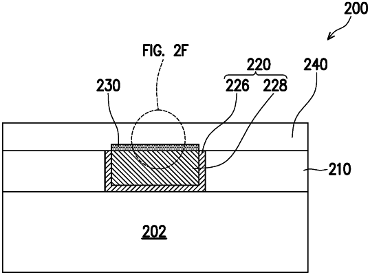
1. A semiconductor structure, comprising:
a substrate;
a first dielectric layer on the substrate, the first dielectric layer comprising a contact structure embedded therein, the contact structure comprising a diffusion barrier including a first metal and a conductive line surrounded by the diffusion barrier and including a second metal different from the first metal;
a self-assembled monolayer on a top surface of the conductive line, but not on a top surface of the diffusion barrier; and
a second dielectric layer on the first dielectric layer and the contact structure,
wherein the self-assembled monolayer is chemically bonded to the conductive line and the second dielectric layer, the self-assembled monolayer derived from a self-assembly molecule having the following formula (I):
X-L-Q (I)
wherein:
X is selenol, isocyanide, carboxylic acid, hydroxaminc acid, phosphonic acid, pyridine, dipyridine or terpyridine;
Q is chlorosilane or trichlorosilicon; and
L is alkylene.
|