| CPC H01L 21/743 (2013.01) [H01L 23/535 (2013.01); H01L 29/66795 (2013.01); H01L 21/3081 (2013.01); H01L 21/3086 (2013.01); H01L 21/31111 (2013.01); H01L 21/31155 (2013.01); H01L 21/76224 (2013.01); H01L 29/785 (2013.01); H10B 10/12 (2023.02)] | 20 Claims |
|
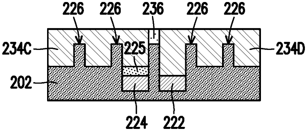
1. A semiconductor device comprising:
a dividing fin protruding from a substrate;
a first buried line on a first side of the dividing fin;
a second buried line on a second side of the dividing fin;
a first gate structure over the first buried line, the first gate structure being electrically coupled to the first buried line;
a second gate structure over the second buried line, wherein a longitudinal axis of the first gate structure is aligned to a longitudinal axis of the second gate structure; and
a first dielectric layer between the second gate structure and the second buried line.
|