| CPC H01L 21/6719 (2013.01) [G01R 31/2831 (2013.01); H01L 21/67115 (2013.01); H01L 21/67248 (2013.01); G01N 19/08 (2013.01); H01L 21/67288 (2013.01)] | 7 Claims |
|
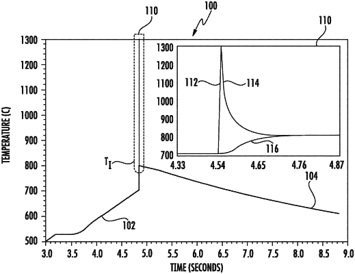
1. A method of determining local contact stress on a substrate resulting from a support structure in a thermal processing system, the method comprising:
obtaining, by one or more processor circuits, a plurality of surface normal estimates for a substrate over a time period;
generating, by the one or more processor circuits, a model specifying a bottom surface profile of the substrate over time based at least in part on the plurality of surface normal estimates; and
determining, by the one or more processor circuits, data indicative of local contact stress at a point of contact between the substrate and a support structure based at least in part on the mode;
modifying thermal processing in the thermal processing system based at least in part on the data indicative of local contact stress.
|