| CPC H01L 21/3083 (2013.01) [H01L 21/0245 (2013.01); H01L 21/02249 (2013.01); H01L 21/3081 (2013.01); H01L 21/8234 (2013.01)] | 20 Claims |
|
1. A method for producing a semiconductor substrate, comprising the following steps:
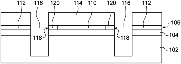
producing a superficial layer arranged on a buried dielectric layer and including a strained semiconductor region, the buried dielectric layer being disposed on a support layer;
producing an etching mask on the superficial layer, covering at least one part of the strained semiconductor region;
etching the superficial layer, buried dielectric layer and support layer according to a pattern of the etching mask, exposing a first lateral edge of the strained semiconductor region;
transforming a portion of the strained semiconductor region, the portion being defined by the first lateral edge on one side and extending into the strained semiconductor region, into a different material, the transformed portion contacting a remaining portion of the strained semiconductor region and having a bottom surface in contact with the buried dielectric layer and an upper surface in contact with the etching mask; and
removing the etching mask.
|