| CPC H01L 21/02507 (2013.01) [H01L 21/02532 (2013.01); H01L 21/02598 (2013.01); H01L 21/8234 (2013.01)] | 27 Claims |
|
1. A method for making a semiconductor device comprising:
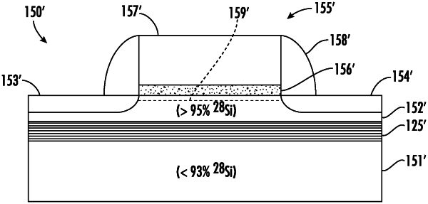
forming a first single crystal silicon layer having a first percentage of silicon 28;
forming a superlattice above the first single crystal silicon layer, the superlattice comprising a plurality of stacked groups of layers, each group of layers comprising a plurality of stacked base silicon monolayers defining a base silicon portion, and at least one non-semiconductor monolayer constrained within a crystal lattice of adjacent base silicon portions; and
forming a second single crystal silicon layer above the superlattice having a second percentage of silicon 28 higher than the first percentage of silicon 28.
|