| CPC H01J 37/32642 (2013.01) [H01J 37/32724 (2013.01); H01L 21/67103 (2013.01); H01L 21/6833 (2013.01); H01L 21/68721 (2013.01); H01L 21/68735 (2013.01); H01J 2237/002 (2013.01); H01J 2237/2007 (2013.01)] | 7 Claims |
|
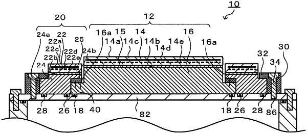
1. A wafer placement device comprising:
a wafer placement stage including a wafer electrostatic chuck and a wafer cooling plate attached to a surface of the wafer electrostatic chuck on side opposite to a wafer placement surface thereof;
a focus-ring placement stage being separate from the wafer placement stage, arranged around the wafer placement stage, and including a focus-ring electrostatic chuck and a focus-ring cooling plate attached to a surface of the focus-ring electrostatic chuck on side opposite to a focus-ring placement surface thereof; and
a clamping member being separate from the focus-ring placement stage and arranged around the focus-ring placement stage,
wherein the wafer cooling plate includes a wafer cooling plate flange projecting radially outward from an outer peripheral surface of an end portion of the wafer cooling plate on a side closer to a mounting plate onto which the wafer placement device is mounted;
the focus-ring cooling plate includes a pressing portion that presses the wafer cooling plate flange against the mounting plate, and a focus-ring cooling plate flange projecting radially outward from an outer peripheral surface of an end portion of the focus-ring cooling plate on side closer to the mounting plate, and
the clamping member is fastened to the mounting plate with fasteners in a state of pressing the focus-ring cooling plate flange against the mounting plate, thus fixing the wafer placement stage and the focus-ring placement stage to the mounting plate without directly fastening the wafer placement stage and the focus-ring placement stage to the mounting plate.
|