| CPC H01H 13/702 (2013.01) [H01H 13/023 (2013.01); H01H 13/14 (2013.01); H01H 13/20 (2013.01)] | 15 Claims |
|
1. A control device, comprising:
a display panel; and
plural key structures located over the display panel, wherein each of the plural key structures comprises:
a keycap, wherein the keycap is light-transmissible;
an optical film layer comprising a light-transmissible region and a supporting region;
an elastic element arranged between the keycap and the optical film layer, wherein the elastic element comprises a support part, a first lateral wall, a first lower part and a hollow part, wherein the support part, the first lateral wall and the first lower part are arranged around the hollow part, the support part is connected with the keycap, and the first lateral wall is arranged between the support part and the first lower part;
plural raised structures formed on the supporting region of the optical film layer and arranged around the light-transmissible region of the optical film layer; and
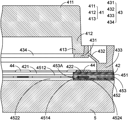
a membrane switch located under the optical film layer, and comprising an upper film layer, a lower film layer and at least one ink layer, wherein the upper film layer comprises a first top surface, a first opening, a first bottom surface and plural first circuit contact points, and the lower film layer comprises a second top surface, a second opening, a second bottom surface and plural second circuit contact points, wherein the first opening runs through the first top surface and the first bottom surface, the first bottom surface faces the lower film layer, and the plural first circuit contact points are formed on the first bottom surface, wherein the second opening runs through the second top surface and the second bottom surface, the second top surface faces the upper film layer, and the plural second circuit contact points are formed on the second top surface, wherein a light beam emitted by the display panel is transmitted upwardly through the second opening, the first opening, the light-transmissible region, the hollow part and the keycap, wherein the at least one ink layer is formed on the first bottom surface or the second top surface, and the upper film layer and the lower film layer are separated from each other through the at least one ink layer, wherein each of the at least one ink layer comprises plural indented regions,
wherein the plural raised structures, the corresponding first circuit contact points, the corresponding indented regions and the corresponding second circuit contact points are aligned with each other along a vertical direction,
wherein when the keycap is pressed down, the keycap or the support part of the elastic element is moved downwardly to push at least one raised structure of the plural raised structures, so that the first circuit contact point corresponding to the pushed raised structure and the second circuit contact point corresponding to the pushed raised structure are contacted with each other.
|