| CPC G11C 11/5671 (2013.01) [G06N 3/065 (2023.01); G11C 16/0483 (2013.01); G11C 16/08 (2013.01); G11C 16/16 (2013.01); G11C 16/24 (2013.01); G11C 16/26 (2013.01); G11C 16/3445 (2013.01); G11C 16/3459 (2013.01); H01L 29/6659 (2013.01); H01L 29/66833 (2013.01); H01L 29/7833 (2013.01); H01L 29/7923 (2013.01); H10B 41/35 (2023.02); H10B 41/41 (2023.02); H10B 43/35 (2023.02); H10B 43/40 (2023.02)] | 18 Claims |
|
1. A method of fabricating a multi-level memory cell, including:
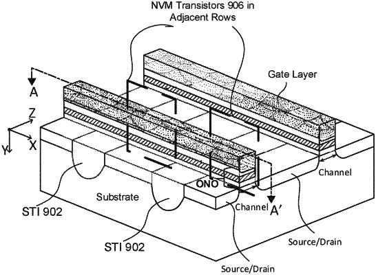
forming at least one shallow trench isolation (STI) in a substrate;
performing a clean and preclean process over the at least one STI and the substrate such that top surfaces of the at least one STI and the substrate are substantially leveled;
forming a tunnel dielectric over the substrate by performing a radical oxidation process;
forming upper and lower silicon oxynitride layers over the tunnel dielectric, wherein an amount of electric charge trapped in the upper and lower silicon oxynitride layers represents N x analog values stored in the multi-level memory cell, wherein N is a natural number greater than 2, and wherein the N x analog values correspond to N x drain current (ID) levels that are linearly incremental and N x threshold voltage (VT) levels that are linearly decremental;
forming a blocking dielectric over the upper and lower silicon oxynitride layers;
patterning the blocking dielectric, the upper and lower silicon oxynitride layers, and the tunnel dielectric to form a memory stack; and
forming a lightly-doped drain extension (LDD) adjacent to the memory stack, wherein the LDD is formed by angled implant such that the LDD extends at least partly under the memory stack.
|