| CPC G11C 11/2275 (2013.01) [G11C 11/221 (2013.01); G11C 11/2259 (2013.01); G11C 11/2273 (2013.01); G11C 11/2255 (2013.01); G11C 11/2257 (2013.01)] | 20 Claims |
|
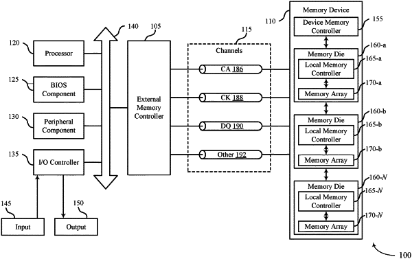
14. A memory device, comprising:
a memory cell;
a switching component coupled to the memory cell;
a sense component coupled to the switching component;
a plurality of storage devices; and
a controller configured to cause the memory device to:
store in each of the plurality of storage devices at correspondingly different times, respective voltage differences between a first voltage and a second voltage associated with a plate line of the memory cell;
provide, to the switching component, a moving average of a voltage difference between the first voltage and the second voltage, based at least in part on the respective voltage differences stored in the plurality of storage devices; and
establish a conductive path between a digit line of the memory cell and the sense component based at least in part on providing the moving average of the voltage difference to the switching component.
|