| CPC G11C 11/221 (2013.01) [G11C 5/10 (2013.01); G11C 11/2255 (2013.01); G11C 11/2257 (2013.01); G11C 11/2293 (2013.01); G11C 11/417 (2013.01); H10B 53/10 (2023.02); H10B 53/20 (2023.02)] | 20 Claims |
|
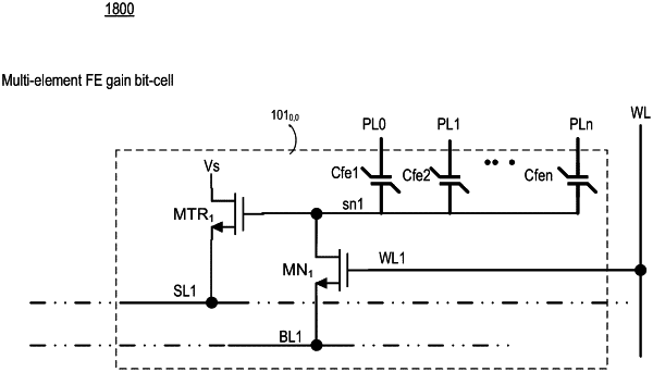
1. An apparatus comprising:
a first node;
a second node;
a first capacitor comprising non-linear polar material, wherein the non-linear polar material is coupled to the first node, and wherein the first capacitor includes a first terminal coupled to a first plate-line;
a second capacitor comprising the non-linear polar material, wherein the non-linear polar material is coupled to the first node, wherein the second capacitor includes a second terminal coupled to a second plate-line, and wherein the non-linear polar material is doped with Mn or Sc;
a first transistor coupled to the first node and a bit-line, wherein the first transistor is controllable by a word-line; and
a second transistor having a gate terminal coupled to the first node, and a source terminal coupled to a select-line and a drain terminal coupled to the second node.
|