| CPC G09G 3/3685 (2013.01) [G09G 3/2018 (2013.01); G09G 3/3614 (2013.01); G09G 3/3648 (2013.01); G09G 2310/0291 (2013.01); G09G 2310/0297 (2013.01); G09G 2310/08 (2013.01); G09G 2320/0209 (2013.01); G09G 2320/0247 (2013.01)] | 20 Claims |
|
1. A display device, comprising:
a display panel which comprises a plurality of data lines including a first data line group and a second data line group, a plurality of gate lines disposed intersecting with the data lines, and display cells as pixels disposed at each intersection of the data lines and the gate lines;
a gate driver which supplies a gate selection signal to each of the gate lines; and
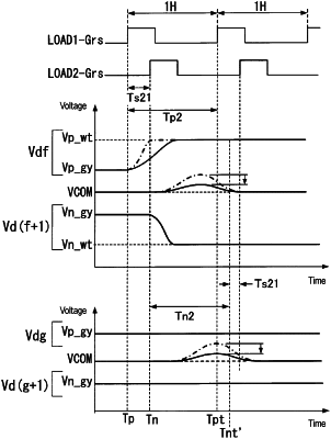
a plurality of data drivers provided for each predetermined number of data lines, wherein each data driver receives an image signal and generates, based on the image signal, a positive gradation data signal higher than a predetermined reference voltage and a negative gradation data signal lower than the predetermined reference voltage, outputs one of the positive gradation data signal and the negative gradation data signal to one data line group of the first data line group and the second data line group, and outputs the other of the positive gradation data signal and the negative gradation data signal to the other data line group of the first data line group and the second data line group,
wherein the data driver:
comprises a plurality of output amplifiers, wherein each output amplifier outputs one of the positive gradation data signal and the negative gradation data signal;
generates a signal as the positive gradation data signal in which a data pulse having a positive voltage value corresponding to a brightness level of each pixel based on the image signal appears in a predetermined cycle, and generates a signal as the negative gradation data signal in which a data pulse having a negative voltage value corresponding to the brightness level of each pixel based on the image signal appears at every predetermined cycle in a phase shifted in a direction delayed with respect to a phase of the positive gradation data signal; and
controls a slew rate of an output amplifier responsible for an output of the positive gradation data signal among the output amplifiers to be lower than a slew rate of an output amplifier responsible for an output of the negative gradation data signal.
|