| CPC G09G 3/3266 (2013.01) [G09G 3/3275 (2013.01); G09G 2310/0278 (2013.01)] | 20 Claims |
|
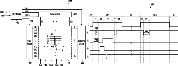
1. A display device comprising:
a pixel that includes a first transistor connected between a first node and a second node to generate a driving current, the pixel connected to a first scan line, a second scan line, a third scan line, a fourth scan line, an emission control line, and a data line;
an emission driver configured to supply an emission control signal having an off-duty corresponding to a first gate-off period and a second gate-off period to the emission control line during a frame period, the first gate-off period corresponding to a first non-emission period and the second gate-off period corresponding to a second non-emission period;
a scan driver configured to supply first, second, third, and fourth scan signals to the first, second, third, and fourth scan lines in the first non-emission period, respectively, and to supply the first scan signal to the first scan line in the second non-emission period;
a data driver configured to supply a data signal to the data line; and
a controller configured to control adjusting of the off-duty of the emission control signal that is a width of each of the first and second non-emission periods in response to a dimming signal, and to control a timing at which the first scan signal is supplied in the second non-emission period.
|