| CPC G09G 3/325 (2013.01) [G09G 3/3275 (2013.01); G09G 2300/0852 (2013.01); G09G 2320/0271 (2013.01); G09G 2320/0633 (2013.01)] | 16 Claims |
|
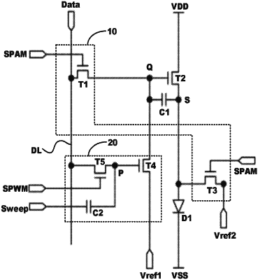
1. A pixel circuit, comprising:
a first transistor;
a pulse amplitude driving module, electrically connected to a gate of the first transistor, configured to drive the first transistor when a middle to high gray value of a frame is being displayed;
a pulse width driving module, electrically connected to the gate of the first transistor, configured to drive the first transistor when a middle to low gray value of the frame is being displayed; and
a data line;
wherein the pulse amplitude module comprises a second transistor and a third transistor, a first electrode of the second transistor is electrically connected to the data line, a gate of the second transistor is configured to receive a pulse amplitude control signal, and a second electrode is electrically connected to the gate of the first transistor; the third transistor has a first electrode configured to receive a first reference signal, a gate configured to receive a pulse amplitude control signal, and a second electrode electrically connected to the second electrode of the first transistor.
|