| CPC G09G 3/3225 (2013.01) [G09G 3/3233 (2013.01); G09G 3/3275 (2013.01); H10K 50/865 (2023.02); H10K 59/121 (2023.02); H10K 59/1213 (2023.02); H10K 59/1216 (2023.02); H10K 59/131 (2023.02); H10K 59/65 (2023.02); H10K 71/00 (2023.02); G09G 2300/0413 (2013.01); G09G 2300/0426 (2013.01); G09G 2300/0819 (2013.01); G09G 2300/0842 (2013.01); G09G 2310/0272 (2013.01); G09G 2310/08 (2013.01); H10K 59/1201 (2023.02); H10K 59/353 (2023.02)] | 20 Claims |
|
1. A display substrate having a mounting region, a first display region adjacent to the mounting region, and a second display region surrounding the first display region and/or the mounting region, the display substrate comprising:
a substrate;
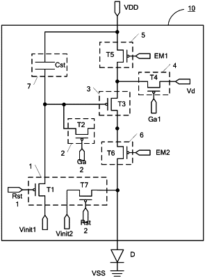
a driving circuit layer on the substrate and comprising a plurality of pixel driving circuits, the plurality of pixel driving circuits being in the first display region and the second display region, and an arrangement density of the pixel driving circuits in the second display region being less than that of the pixel driving circuits in the first display region;
a plurality of light emitting devices in the mounting region, the first display region, and the second display region, a first electrode of each light emitting device being electrically coupled to a corresponding one of the pixel driving circuits, and the pixel driving circuit electrically coupled to the first electrode of the light emitting device in the mounting region being located in the first display region; and
a plurality of data lines in the first display region and the second display region, each pixel driving circuit being electrically coupled to a corresponding one of the data lines,
wherein at least part of the plurality of data lines includes a bend line,
wherein at least one of the data lines which is the bend line is a first data line; the first data line comprises a first sub data line segment directly coupled to the pixel driving circuit for driving at least part of the light emitting devices in the mounting region, and a second sub data line segment directly coupled to the pixel driving circuit for driving at least part of the light emitting devices in the second display region; and the first sub data line segment and the second sub data line segment are at least partially not on a same straight line.
|