US 11,810,485 B2
Electronic device
Chin-Lung Ting, Miao-Li County (TW); Chung-Kuang Wei, Miao-Li County (TW); Li-Wei Mao, Miao-Li County (TW); Chi-Liang Chang, Miao-Li County (TW); and Chia-Hui Lin, Miao-Li County (TW)
Assigned to InnoLux Corporation, Miao-Li County (TW)
Filed by InnoLux Corporation, Miao-Li County (TW)
Filed on Dec. 6, 2022, as Appl. No. 18/075,434.
Application 17/161,617 is a division of application No. 16/362,676, filed on Mar. 24, 2019, granted, now 10,957,226, issued on Mar. 23, 2021.
Application 18/075,434 is a continuation of application No. 17/567,176, filed on Jan. 3, 2022, granted, now 11,551,587.
Application 17/567,176 is a continuation of application No. 17/161,617, filed on Jan. 28, 2021, granted, now 11,250,738, issued on Feb. 15, 2022.
Claims priority of provisional application 62/660,222, filed on Apr. 19, 2018.
Claims priority of application No. 201811103070.4 (CN), filed on Sep. 20, 2018.
Prior Publication US 2023/0102366 A1, Mar. 30, 2023
This patent is subject to a terminal disclaimer.
Int. Cl. G09F 9/302 (2006.01); G09G 3/32 (2016.01)
CPC G09F 9/3026 (2013.01) [G09G 3/32 (2013.01); G09G 2300/026 (2013.01)] 7 Claims
OG exemplary drawing
 
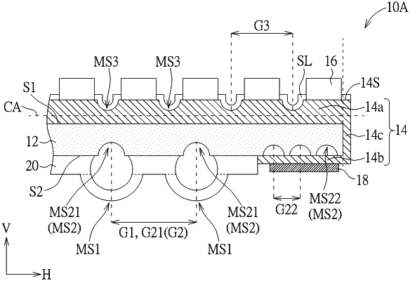
1. An electronic device, comprising:
a substrate having a plurality of structures;
a circuit layer disposed on the substrate; and
a plurality of diodes disposed on the circuit layer;
wherein a first spacing is defined as a distance between a center point of a first one of the structures and a center point of a second one of the structures, a second spacing is defined as a distance between a center point of a third one of the structures and a center point of a fourth one of the structures, and an absolute value of a difference between the first spacing and the second spacing is less than 0.5 times radius of curvature of the electronic device when the electronic device is bent.