| CPC G06F 3/0611 (2013.01) [G06F 3/0619 (2013.01); G06F 3/0634 (2013.01); G06F 3/0659 (2013.01); G06F 3/0673 (2013.01); G06F 12/0607 (2013.01); G11C 5/04 (2013.01); G11C 7/10 (2013.01)] | 20 Claims |
|
1. A buffer circuit, comprising:
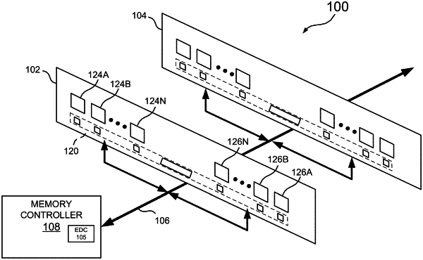
a primary interface for coupling to a group of links associated with a memory controller, the primary signaling interface operating at a primary data signaling rate;
a secondary interface including a first signal path for coupling to a first memory device, and a second signal path for coupling to a second memory device, the first and second signal paths operating at a secondary data signaling rate;
wherein during a first mode of operation, the primary data signaling rate is at least twice the secondary data signaling rate, and wherein a first time interval associated with a transfer of first information via the first signal path temporally overlaps a second time interval involving second information transferred via the second signal path.
|