| CPC G06F 3/0445 (2019.05) [B29C 51/002 (2013.01); B29C 51/14 (2013.01); B29K 2995/0005 (2013.01); B29K 2995/0006 (2013.01); B29K 2995/0026 (2013.01); B29L 2031/3475 (2013.01); G06F 2203/04103 (2013.01)] | 43 Claims |
|
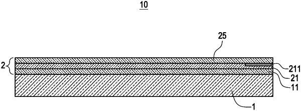
1. A transparent conductive substrate structure used for a thermoforming process, and the transparent conductive substrate structure comprising:
a transparent cover plate comprising a toughening layer on one side or two sides of a surface of the transparent cover plate, and
a touch sensing layer structure arranged on one surface of the toughening layer, and the touch sensing layer structure comprising:
a first transparent conductive layer directly arranged on the toughening layer, and a first wiring area arranged on one side of a surface of the first transparent conductive layer, and a first electrode wire layer arranged on a surface of the first wiring area, and
a buffer protective layer arranged on the other surface of the first transparent conductive layer,
wherein, a thickness of the toughening layer is less than or equal to 3 μm, and a surface of the toughening layer is treated with plasma to increase adhesion between the toughening layer and the first transparent conductive layer.
|