US 11,809,126 B2
Charging member, charging device, process cartridge, and image forming apparatus
Yasuhiko Kinuta, Kanagawa (JP); Yuki Tagawa, Kanagawa (JP); Ken Ozaki, Kanagawa (JP); and Noboru Hirakawa, Kanagawa (JP)
Assigned to FUJIFILM Business Innovation Corp., Tokyo (JP)
Filed by FUJIFILM Business Innovation Corp., Tokyo (JP)
Filed on Jan. 24, 2022, as Appl. No. 17/582,008.
Claims priority of application No. 2021-135201 (JP), filed on Aug. 20, 2021.
Prior Publication US 2023/0068161 A1, Mar. 2, 2023
This patent is subject to a terminal disclaimer.
Int. Cl. G03G 15/02 (2006.01); G03G 21/18 (2006.01); G03G 5/047 (2006.01); G03G 5/147 (2006.01); C08K 3/04 (2006.01); C08L 15/02 (2006.01); C08K 3/013 (2018.01)
CPC G03G 21/1814 (2013.01) [C08K 3/04 (2013.01); C08L 15/02 (2013.01); G03G 5/047 (2013.01); G03G 5/147 (2013.01); C08K 3/013 (2018.01); C08K 2201/001 (2013.01)] 20 Claims
OG exemplary drawing
 
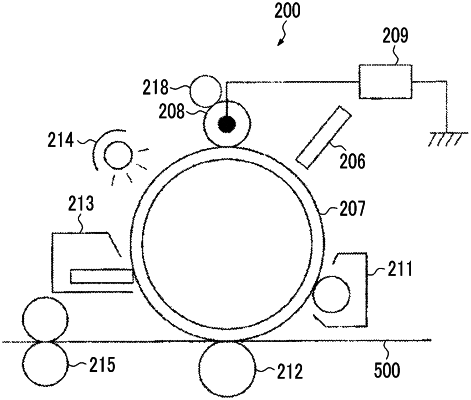
1. A charging member comprising:
a conductive base material;
an elastic layer that is provided on the conductive base material and has a storage elastic modulus G of 5.0 MPa or less at 100 Hz; and
a surface layer that is provided on the elastic layer,
wherein, in a Cole-Cole plot obtained by measuring the charging member in a range of 1 MHz to 0.1 Hz by an alternating current impedance method, a resistance component Ra of a capacitive semicircle including 2.5 kHz is 6.3×10⁴Ω or less.