| CPC G03F 7/70358 (2013.01) [G03F 7/70433 (2013.01); G03F 7/70525 (2013.01)] | 20 Claims |
|
1. A method, comprising:
generating, by a scanner control system, an exposure recipe for performing an exposure operation for a semiconductor substrate,
wherein the exposure recipe includes information identifying:
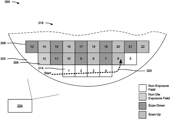
a plurality of die exposure fields, on the semiconductor substrate, that are to be exposed in the exposure operation,
a plurality of non-exposure fields, on the semiconductor substrate, for which exposure is to be skipped in the exposure operation, and
a scanner route for traversing across the plurality of die exposure fields and a first non-exposure field of the plurality of non-exposure fields,
wherein a second non-exposure field of the plurality of non-exposure fields is omitted from the scanner route; and
providing, by the scanner control system, an input to a substrate stage of an exposure tool to cause the substrate stage to step the semiconductor substrate along the scanner route in the exposure operation.
|