| CPC G03F 1/82 (2013.01) [B08B 7/0035 (2013.01); B08B 7/0071 (2013.01); G03F 7/70033 (2013.01); G03F 7/70733 (2013.01); G03F 7/70925 (2013.01); H01L 21/67028 (2013.01); H01L 21/67225 (2013.01)] | 20 Claims |
|
1. A method of manufacturing a semiconductor structure, comprising:
receiving a semiconductive substrate;
inspecting a photomask prior to applying the photomask in an exposure operation on the semiconductive substrate;
performing the exposure operation on the semiconductive substrate in a first chamber by using the photomask when the photomask passing the inspection; and
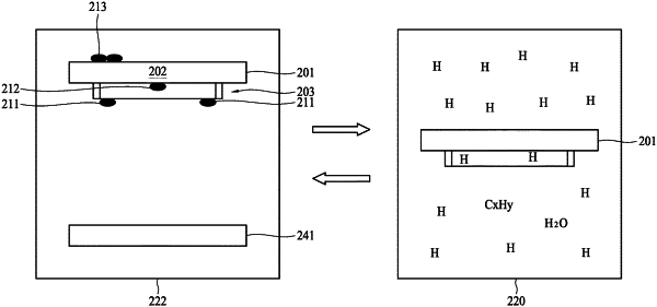
performing a cleaning operation on the photomask in a second chamber when the photomask fails to pass the inspection, wherein the cleaning operation comprises:
providing hydrogen radicals to the second chamber; and
removing carbon-containing contaminants and oxygen-based contaminants on the photomask by having the hydrogen radicals reacting with the carbon-containing contaminants and the oxygen-based contaminants.
|