| CPC G02F 1/133305 (2013.01) [G02F 1/133308 (2013.01); G02F 1/133548 (2021.01)] | 10 Claims |
|
1. An electromagnetic wave emitting structure, comprising:
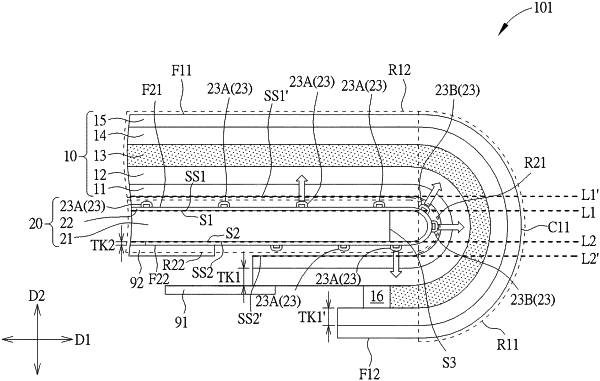
a substrate having a first flat part and a foldable part connected with the first flat part;
a plurality of electromagnetic wave emitting units disposed on the substrate, wherein two adjacent ones of the plurality of electromagnetic wave emitting units on the first flat part have a first pitch in a first direction parallel to a surface of the first flat part, another two adjacent ones of the plurality of electromagnetic wave emitting units on the foldable part have a second pitch in a second direction parallel to a surface of the foldable part, and the second pitch is different from the first pitch; and
a circuit structure electrically connected with the plurality of electromagnetic wave emitting units, wherein in a normal direction of the first flat part, the circuit structure overlaps the plurality of electromagnetic wave emitting units on the first flat part, and the circuit structure comprises a printed circuit board, a tap carrier package structure, or a chip on film structure.
|