| CPC G02B 6/4251 (2013.01) [G02B 6/12002 (2013.01); G02B 6/12004 (2013.01); H01L 25/167 (2013.01); G02B 6/12 (2013.01); G02B 2006/121 (2013.01); G02B 2006/12061 (2013.01); H01L 23/562 (2013.01)] | 20 Claims |
|
1. A photonic integrated circuit, comprising:
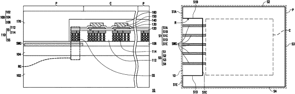
a substrate comprising a top layer made of a semiconductor material;
an interconnection layer over the substrate, wherein the interconnection layer comprises a seal ring structure and an interconnection structure surrounded by the seal ring structure, the seal ring structure has at least one recess from a top view, the recess concaves towards the interconnection structure, and the seal ring structure is a continuous structure from the top view; and
a plurality of silicon waveguides embedded in the top layer of the substrate.
|