| CPC G02B 6/4215 (2013.01) [G02B 6/4206 (2013.01)] | 20 Claims |
|
1. A method for forming an optical coupler, comprising:
forming an insulation layer on a semiconductor substrate;
epitaxially growing a semiconductor material on the insulation layer to form a semiconductor layer;
etching the semiconductor layer to form an array of etched regions in the semiconductor layer according to a predetermined pattern; and
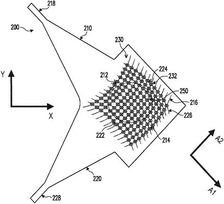
depositing a dielectric material into the array of etched regions to form an array of scattering elements in the semiconductor layer, wherein the scattering elements are arranged at a plurality of intersections of a first set of concentric elliptical curves crossing with a second set of concentric elliptical curves rotated proximately 90 degrees to form a two-dimensional (2D) grating, wherein
each scattering element is a pillar in a corresponding one of the etched regions, and
the pillar has a top surface whose shape is a concave polygon having at least 8 edges.
|