| CPC G02B 6/4215 (2013.01) [G02B 6/3572 (2013.01); G02B 6/4224 (2013.01)] | 18 Claims |

|
1. A device comprising:
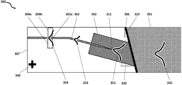
first, second and third elements fabricated on a common substrate;
wherein the first element comprises an active waveguide structure comprising electrically pumped optical source supporting a first optical mode, the second element comprises a passive waveguide structure supporting a second optical mode in at least part of the second element, and the third element, at least partly butt-coupled to the first element, comprises an intermediate waveguide structure supporting intermediate optical modes;
wherein at least part of the second element supports at least one optical mode that interacts with rare-earth dopants;
wherein a tapered waveguide structure in at least one of the second and third elements facilitates efficient adiabatic transformation between the second optical mode and at least one of the intermediate optical modes;
wherein no adiabatic transformation occurs between any of the intermediate optical modes and the first optical mode; and
wherein mutual alignments of the first, the second, and the third elements are defined using lithographic alignment marks that facilitate precise alignment between layers formed during processing steps of fabricating the first, the second, and the third elements.
|