| CPC G02B 5/20 (2013.01) [B29D 11/00634 (2013.01)] | 18 Claims |
|
1. An optical element, comprising:
a first substrate;
a second substrate, disposed opposite to the first substrate;
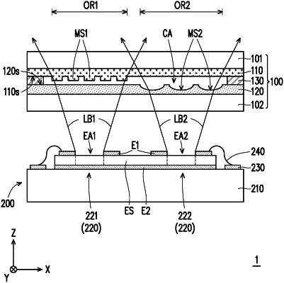
a first optical film, disposed on the first substrate, the first optical film has a first surface and a plurality of first optical microstructures, the first optical microstructures are disposed on the first surface;
a second optical film, disposed on the second substrate, wherein the second optical film has a second surface and a plurality of second optical microstructures, the second surface is opposite to the first surface, the second optical microstructures are disposed on the second surface, and the orthogonal projection of the first optical microstructures on the first substrate does not overlap with the orthogonal projection of the second optical microstructures on the first substrate; and
a spacer, disposed between the first substrate and the second substrate, wherein the spacer directly contacts the first optical film and the second optical film, the first surface, the second surface and the spacer define a cavity of the optical element, and the first optical microstructures and the second optical microstructures are disposed in the cavity.
|