| CPC G01R 31/2893 (2013.01) [G01R 31/2891 (2013.01)] | 25 Claims |
|
1. A method for testing at least one single chip in a wafer probing system, at least comprising:
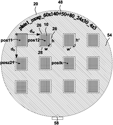
providing an adapter plate having an interface surface for contacting a vacuum chuck of the wafer probing system, the adapter plate being configured to accommodate the at least one single chip in a cutout with a chip rear surface being flush with the interface surface;
loading the adapter plate with the at least one single chip into the wafer probing system;
reading an identification data of the loaded adapter plate;
storing the identification data of the loaded adapter plate in a controller of the wafer probing system;
moving the vacuum chuck together with the adapter plate to a predefined search area for probes of the wafer probing system;
determining an exact position of the at least one single chip in the adapter plate in the search area;
adjusting the position of the vacuum chuck until a front surface of the at least one single chip is in an operational region for being contacted by the probes of the wafer probing system;
adding the adjusted position of the vacuum chuck corresponding to the at least one single chip positioned in the operational region to the stored identification data of the loaded adapter plate;
contacting the at least one single chip electrically with probes of the wafer probing system; and
testing the at least one single chip with test routines stored in a controller of the wafer probing system,
wherein chip parameters, in particular a chip position and/or a rotation angle on the adapter plate, are acquired in a determination phase of a positioning algorithm, and further comprising:
defining a pattern on a front surface of the at least one single chip which is suitable for adjusting the position and/or the rotation angle of the at least one single chip,
wherein at least one search area is defined for finding a match of the pattern with the position of the at least one single chip.
|