| CPC G01R 29/26 (2013.01) [G01R 31/31709 (2013.01); H03K 19/01855 (2013.01); H03L 7/07 (2013.01); H03L 7/08 (2013.01); G01R 29/0276 (2013.01)] | 20 Claims |
|
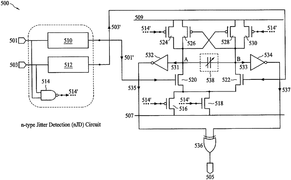
1. A noise detection circuit, comprising:
a first component configured to receive a clock signal;
a second component configured to receive a reference clock signal, wherein the first and second components each comprises an n-type metal-oxide-semiconductor (NMOS) field-effect-transistor (FET);
a latch circuit, coupled to the first component at a first node and coupled to the second component at a second node, and configured to latch logic states of voltage levels at the first and second nodes, respectively, based on a timing difference between transition edges of the clock signal and the reference clock signal; and
a plurality of capacitors coupled between the first and second nodes.
|