| CPC G01N 27/4145 (2013.01) [B01F 31/85 (2022.01); B01F 33/30 (2022.01); B01F 33/3045 (2022.01); B01L 3/502707 (2013.01); B01L 3/502715 (2013.01); B01L 3/502761 (2013.01); B01L 3/502792 (2013.01); G01N 33/5438 (2013.01); H10N 30/1051 (2023.02); H10N 30/2042 (2023.02); H10N 30/2047 (2023.02); B01L 2200/12 (2013.01); B01L 2300/06 (2013.01); B01L 2300/0645 (2013.01); B01L 2300/0663 (2013.01); B01L 2300/0819 (2013.01); B01L 2300/0887 (2013.01); B01L 2300/1827 (2013.01); C12Q 1/6825 (2013.01)] | 20 Claims |
|
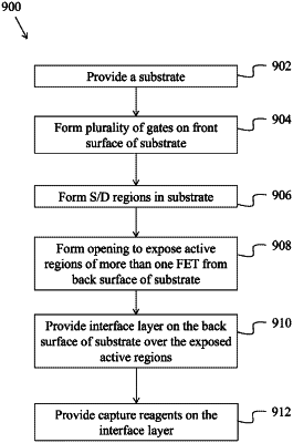
1. A method of fabricating a semiconductor device, the method comprising:
forming a plurality of bio-field effect transistor (bioFET) sensors on a semiconductor substrate with a first surface and a second surface opposite to the first surface, wherein forming each bioFET sensor of the plurality of bioFET sensors comprises:
forming a gate on the first surface of the semiconductor substrate, wherein the gate is formed over a first channel region in the semiconductor substrate, and
forming a first pair of source/drain (S/D) regions in the semiconductor substrate on either side of the first channel region;
forming a plurality of access FETs on the semiconductor substrate, wherein forming each access FET of the plurality of access FETs comprises:
forming an access gate on the first surface of the semiconductor substrate, wherein the access gate is formed over a second channel region in the semiconductor substrate, and
forming a second pair of S/D regions in the semiconductor substrate on either side of the second channel region;
forming an isolation layer on the second surface of the semiconductor substrate;
forming an opening in the isolation layer, wherein the opening exposes the first channel regions of more than one bioFET sensor of the plurality of bioFET sensors and does not expose the second channel regions of the plurality of access FETs; and
disposing a continuous interface layer on the isolation layer and within the opening over the first channel regions of the more than one bioFET sensor, wherein the continuous interface layer extends over the second channel regions of the plurality of access FETs.
|