| CPC G01M 11/081 (2013.01) [G01L 1/248 (2013.01); G01M 5/0008 (2013.01)] | 12 Claims |
|
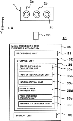
1. A stress distribution image processing device comprising:
a memory storing a program; and
a processing unit,
wherein the program, when executed by the processing unit, causes the processing unit to:
designate a normalization region which includes a portion of stress equal to or larger than a predetermined threshold value in a screen of a stress distribution image of a target object; and
obtain a normalized image of stress distribution by normalizing pixels in the normalization region based on stress values in the normalization region, by utilizing a normalization method using a maximum stress value and a minimum stress value of the pixels in the normalization region.
|