| CPC G01F 1/3209 (2013.01) [G01F 1/3287 (2022.01)] | 19 Claims |
|
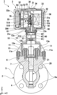
1. A field device comprising:
a casing portion that has an amplifier shield chamber into which an analog signal transfer portion transferring an analog signal output from a detector is able to be inserted;
a signal conversion portion that is disposed inside the amplifier shield chamber, the signal conversion portion being configured to convert the analog signal into a digital signal;
a first connector that is disposed inside the amplifier shield chamber, the first connector being configured to connect the analog signal transfer portion and the signal conversion portion to each other in an attachable/detachable manner;
a communication hole through which the inside and the outside of the amplifier shield chamber communicate with each other;
a first substrate portion that comprises:
a main body portion which is disposed inside the casing portion and outside the amplifier shield chamber; and
an insertion portion which extends from the main body portion and is inserted into the amplifier shield chamber through the communication hole; and
an amplifier shielding plate that closes the communication hole through which the first substrate portion has passed.
|