| CPC C23C 14/5813 (2013.01) [C23C 14/086 (2013.01); C23C 14/28 (2013.01); H01B 5/14 (2013.01)] | 5 Claims |
|
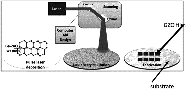
1. A method of producing gallium-doped zinc oxide films with enhanced conductivity, the method comprising:
depositing a gallium-doped zinc oxide film on a substrate using a pulsed laser deposition technique; and
subjecting the deposited gallium-doped zinc oxide film to a post treatment comprising subjecting the deposited gallium-doped zinc oxide film to an ultraviolet laser beam resulting in recrystallization in the deposited gallium-doped zinc oxide film,
wherein the recrystallization results in a recrystallized gallium-doped zinc oxide film with a conductivity higher than the conductivity of the gallium-doped zinc oxide film deposited on the substrate using the pulsed laser deposition technique, and
wherein the recrystallized gallium-doped zinc oxide film contains a recrystallized grain structure on its surface, wherein grains of the film contain nanoparticles, and grain boundaries between the nano particles of the grains are faceted, and wherein the film has an average surface roughness in the range of 0.9-2.5 nm.
|